The Basics of Logic Circuits – Part 1
An Introduction
As a child I had an interest in electronics. I took options at school which taught me the basics, but found that a few small details were omitted which made it slightly more difficult to move from theory to practice. Following a recent discussion with my brother about how we thought it would be best to introduce electronics to a beginner and move through to designing and building your own circuits, I decided to write something to hopefully help other people in the same position as my 15 year old self.
Useful Parts for the Following
- 74HC00 – Quad 2-input NAND gate
- 74HC04 – Hex inverter gate (NOT)
- 74HC32 – Quad 2-input OR gate
- 74HC08 – Quad 2-input AND gate
- 2N7000 – MOSFET
- Pushbutton
- LED
- 220R Resistor
- Breadboard
- Power source?
Basic Boolean Logic
As a tool for introducing electronics in more general terms, I’m going to introduce logic and logic chips. In electronics, logic is usually based on the theory of using voltages to represent two states, “TRUE” or “FALSE”, sometimes called “HIGH” and “LOW” (in reference to the voltage). When the voltage is high, and the signal is considered to be present, this is a TRUE. Multiple TRUE and FALSE signals can be used together representing a set of inputs to be analysed to give specific outcomes in specific input scenarios by applying various logic operations. Even with basic logic rules, complex systems can be built.
The three most basic logic operations commonly seen in electronics are “AND”, “OR” and “NOT”. These are implemented physically as “gates” (e.g. “you need an AND Gate in your circuit”), which it is common to find several of in one microchip. The most conceptually simple gate is the NOT gate, which takes an input signal, and inverts it before outputting it. This means that when applying a logic TRUE to a NOT gate, it will produce a logic FALSE at the output pin and vice versa. The OR gate provides a logic TRUE when either one, the other, or both of its inputs are TRUE. Finally, the AND gate produces a logic TRUE only when both inputs are TRUE. Any time the output is not TRUE for any of these gates, it will be FALSE. The following table shows all combinations for two inputs named Input A and Input B. It is possible to have AND and OR gates with more inputs, although the same result can be achieved by using multiple gates consecutively and feeding the output of one into the input of another. Note that as shown in the following table, the NOT gate has a single input. Within the table, the NOT gate has been assumed to be connected to Input A (and duplicate second rows have been omitted for clarity).
| Input A | Input B | AND | OR | NOT |
| FALSE | FALSE | FALSE | FALSE | TRUE |
| FALSE | TRUE | FALSE | TRUE |
|
| TRUE | FALSE | FALSE | TRUE | FALSE |
| TRUE | TRUE | TRUE | TRUE |
|
Equivalent Circuits
The various logic circuits can be considered as behaving in a similar manner to the following conventional electrical equivalents. These equivalents use switches to achieve the same behaviour, where the bulb represents the output.
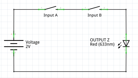
AND – Two Switches in a Row
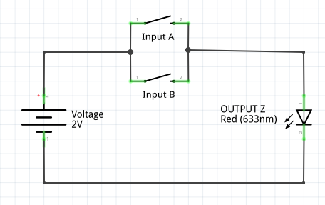
OR – Two Switches in Parallel
NOT – A switch in Parallel with the Load
When the switch is pressed, the load is bypassed as the path of least resistance is through the closed switch. This means that when the switch is closed (TRUE), the LED is off (FALSE) and vice versa. The resistor R1 is included so that the switch is not a dead short over the battery. The battery voltage was increased to 5V to make the circuit more realistic in that the LED would be dim (or go out) if the 2V supply from the two previous circuits was used.
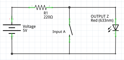
If you are unsure why this circuit acts as a NOT, consider that the resistance of a typical 10cm wire and switch might be 0.0005 ohm. Current follows alternative paths inversely proportionally to the resistance. If two paths are of equal resistance, the current will divide equally between both routes. If one resistance is 10 time greater than the other, 10 times more current will flow through the LOWER resistance path. As the LED has an effective resistance tens of thousands of times greater than the wire (if not more) effectively all the available current will go through the wire and switch rather than the LED. When the switch is released (goes open) the resistance of that path becomes huge (it might as well be infinite) and so all available current goes through the LED as it is now the path of least resistance. Much more detail can be given regarding how the resistance of an LED changes depending on voltage, about the resistance of the circuit and about the resistance of individual parts of the circuit etc. but very quickly this gets too detailed and distracts from the purpose of this example!
Just Draft Notes from here on in. Also, check that a 1k resistor is suitable for the circuit I drew. OK – I’ve checked the 1k and it looks OK (but I’d prefer to test the circuit) It results in less than 1.4mA current in the LED and not more than 5mA into the Base? something like that. A bigger resistor might be better, say 2 or even 3k.
Using Transistors Instead of Switches
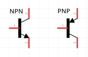
There are two main types of Transistors, NPN and PNP. Effectively, the NPN produces switches on when a current is provided to the Base pin, while a PNP switches off when a current is provided to the Base pin. I remember the difference between the two symbols by telling myself that NPN stands for “Not Pointing iN”, with reference to the arrow in the symbol. The two symbols are as follows.
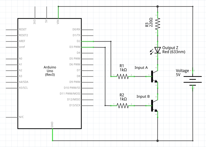
AND – Using Two NPN Transistors
In the preceding example the Base pins on the transistors are shown with the Base pins protected by 1k current limiting resistors (R1 and R2). In a real application, these inputs would be connected to something like the output pins of a microcontroller. The LED is also in line with a 220R current limiting resistor. To implement this circuit, you might use the common BC547 NPN transistor. This would be suitable for use with, for example, a 5V Arduino Uno. The following schematic shows how this might be implemented. Similar methods can be used for the OR and NOT implementations which follow, but this post does not go into detail regarding using transistors as the primary intention is to explain the use of Logic chips. I might return to the subject of transistors at a later date.
OR – Using NPN Transistors
Supplying current to either (or both) Input A or B will provide a current path from the LED to ground, completing the circuit and implementing our OR logic.
NOT – Using a PNP Transistor
To implement the NOT logic using a transistor, the easiest solution is to use a PNP transistor instead of the NPN used in the previous two examples. As noted, this type of transistor closes when current is provided to the Base. Note the different location of the arrow within the transistor’s symbol. The common PNP equivalent of the BC547 is the BC557.
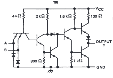
In reality, within integrated circuits, the logic implementations are more complex to allow greater flexibility and a more well rounded product. The following is an extract from a Texas Instruments datasheet for the 7408, showing the individual transistors within each gate of the logic chip. The design is beyond me… especially as I’ve never seen a transistor with 4 legs.
Additionally, it is also possible to implement logic using “Relay Logic”, but that is a topic for another day.
Symbols
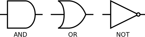
The symbols for the AND, OR and NOT gates are shown above. Note the small dot on the NOT gate – without the dot the triangular symbol would represent a buffer, which does not modify the output logic and simply passes the input signal to the output. The dot symbolises that the output should be inverted. This dot can be also added to other gates to mean that the output should be inverted. In the case of the AND and OR gates, this produces the NAND and NOR gates.
Note that schematics within this post were drawn using Fritzing – a free circuit designing program for Linux, MacOS and Windows.