Upgrading My Acorn A3010
I also made this page, to help someone install the DualClock board in their A3010.
Background and Repair
I don’t remember exactly when, but at some point around 2000 my parents got me an A3010. I didn’t have any software for it beyond what was in ROM and didn’t really know anybody with an Acorn, so I basically just used it as a faster BBC Micro, especially as it had an Analogue / Userport podule in it and I was starting to get into electronics (slowly) during my later teens.
I used it intermittently for a few years, until I left home and couldn’t easily take it with me for the first few years.
Later, I had it in the house but hadn’t really done much with it other than test it once to check it worked. After that, I hadn’t used it for a few years when a collogue warned me that the batteries caused serious damage (in about 2014). I went home and pulled it to bits to find green corrosion and a dead battery. I cut the battery out and cleaned it as best as I could with IPA. The trace damage didn’t look like something I knew how to repair so I sadly packed it away hoping to work out what to do at some point. At least the battery was out of it.
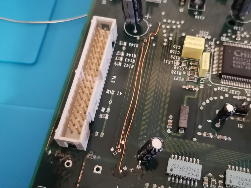
The year : 2021 – the world is in disarray as a pandemic sweeps the earth and I had accidentally bought a dead, battery damaged Macintosh IIx… and was surprised to discover that it turns out I am now comfortable doing trace repairs. I’d also picked up an ultrasonic cleaner and decided to take the chance to clean up and have a look at the poor A3010. Looking at the board again, I found that it wasn’t as bad as I thought and a small number of trace repairs later and a clean, and I had it up and running. (Note that the traces to the parallel port are not in great condition, but do all conduct. I may return to tidy them up a bit at a later date, by re-tinning and covering with fresh soldermask).
Upgrades
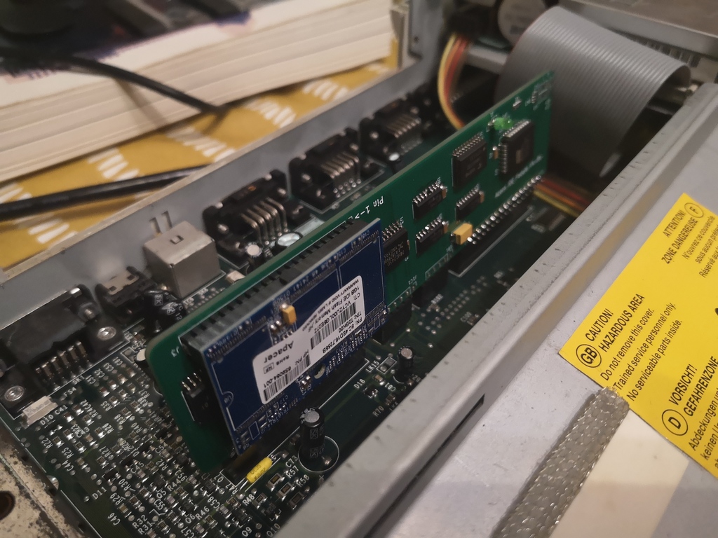
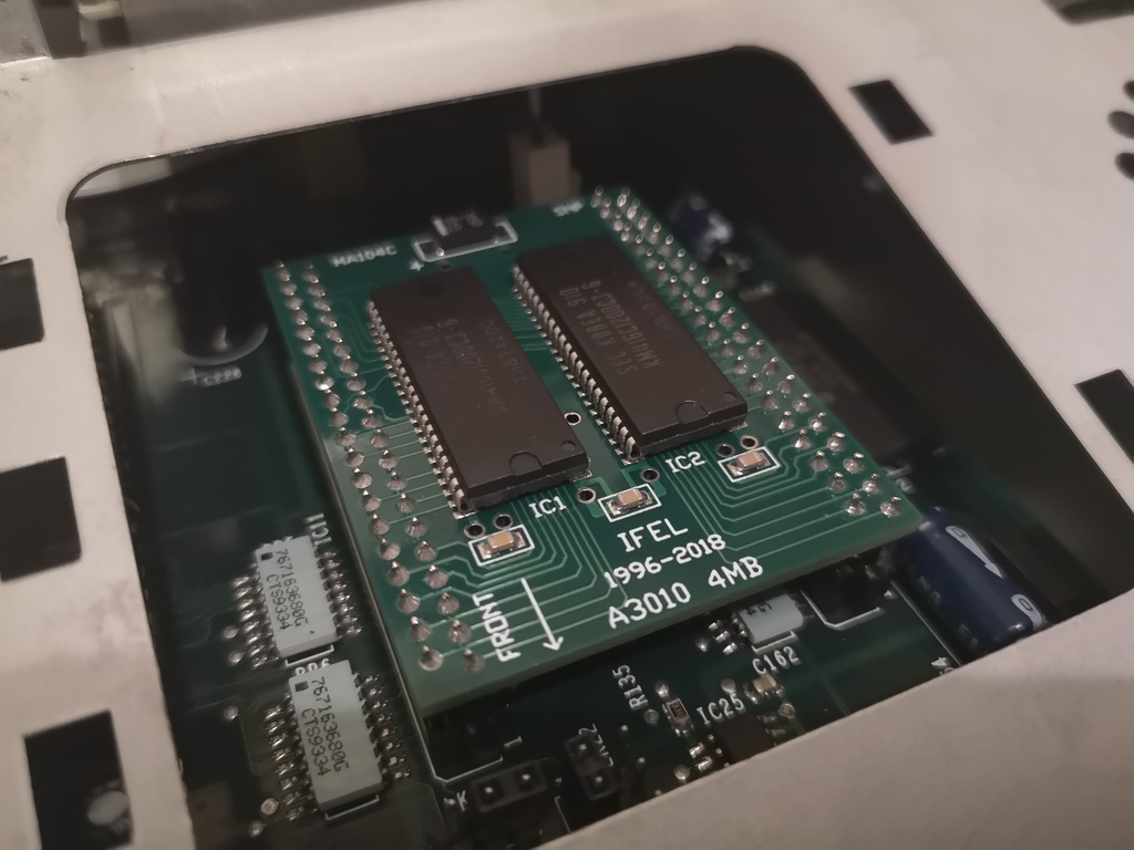
Excited to have a working Acorn, I decided to upgrade it to say sorry for abandoning it for years. I bought a Gotek, IDE card from IanS and 4MB of RAM. Further investigation found mentions of quite significant overclocks being possible, especially when using a fast 4MB RAM upgrade, as this disables the onboard RAM.
Overclocking
The description of the overclock explained how, but not why this was possible, which made me a little uncomfortable so I decided to investigate. Why is it possible to overclock some (not all easily – some do not have the unpopulated footprint for an additional clock) A3010s by just adding an additional clock and a resistor?
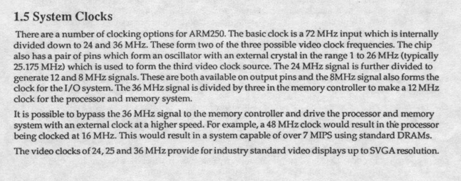
The following extract from the ARM250 datasheet was interesting as it describes the standard configuration for an A3010 – the 72MHz clock is divided by 2, and then again by 3, to produce the 12MHz for the processor and for the memory. The next paragraph then goes on to explain that it is possible to use an alternative clock source and even references running the chip at 16Mhz (with no warnings or statements that “this is not advised”).
Further into the datasheet, there is a description of pin functions for the ARM250 that includes a description of “sysclk”. This is the optional input described above, and the description explains why this pin makes overclocking so trivial.
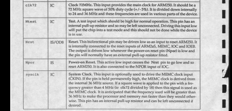
Apparently, the act of connecting an active clock in the correct speed range alone is enough to cause the ARM250 to automatically detect it, and switch clock source from clk72 (divided by 6) to sysclk (divided by 3). If no signal is detected and the pin is held high, it switches back to clk72. There is even conveniently a pullup on the pin so if left unconnected (as by default on the A3010) it is pulled high and disabled.
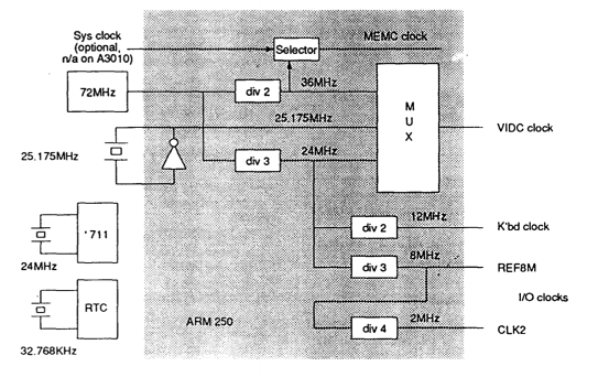
The following drawing also helps understand how everything works, showing how the chip is able to select from two sources, and where the dividers sit.
Next I pulled out various related schematics I had, some using sysclk and some only clk72. It should be noted that, firstly, the mezzanine A3010 is implemented in a slightly different way because they do not derive the clock by dividing by 6. Documentation states that this was done to avoid expensive clock dividers. Secondly, my A3010 is a later board revision and frustratingly does not match either schematic. The following is the mezzanine A3010 design. This variant uses sysclk, but it only implements a divide by 2. Note also that Clk72 is only 36MHz instead of the obvious 72MHz. This is due to the cost optimisation. Note that between the Clock X3 and sysclk a 33R resistor has been placed in line – make a note of this. Ignore that the mezzanine board is confusingly labelled “ARM250”.
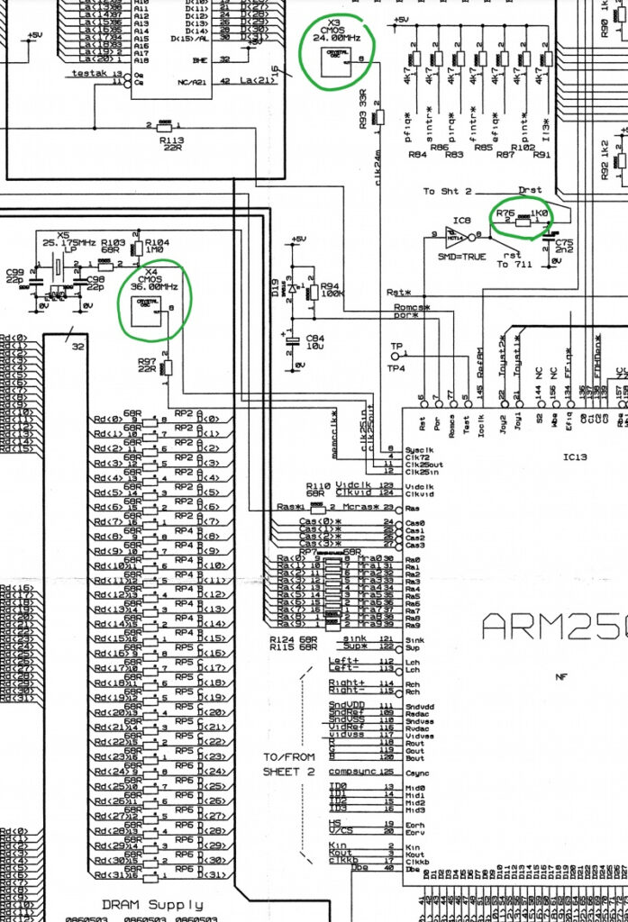
The following schematic extract is for the intermediate age A3010 which used the ARM250 chip rather than the mezzanine board.
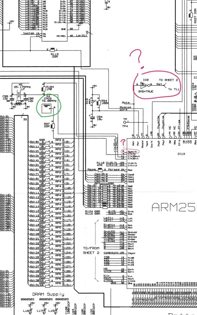
Here we can see sysclk is completely unconnected and X4, connected to clk72, is a 72MHz crystal showing that now, in line with the normal operation of the ARM250, the processor clock is one sixth of clk72. On boards of this design (with no footprint for a clock connected to the sysclk pin), modifications are still possible, but more complex. It would be necessary to tack a wire onto the processor pin, find ground and 5v and then wire in a resistor and a clock. Not impossible… but care would need to be taken.
Finally, the following is a schematic for the A3020. This schematic shows an implementation using an ARM250 (not a mezzanine board), but, with a position for sysclk.
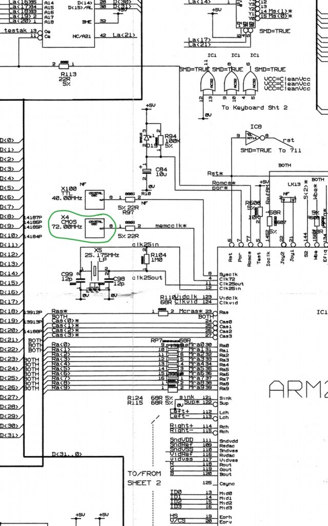
Note two things here 1) while overclocking is likely possible by placing a fast clock at location X100, for a significant overclock I suspect it would be necessary to replace the RAM soldered on the motherboard with faster chips and 2) the clock shown in the schematic is 40MHz meaning that a machine built as above would be 13.3333MHz?! I anticipate that on machines that were sold, no clock was fitted at this location on the A3020, possibly confirmed by photos at BeebMaster and Chris’ Acorns.
The most interesting thing for me about this A3020 schematic is that this section more closely matches my A3010 than either of the A3010 schematics. Note here that the resistor located in line with the clock signal, between sysclk and X100 is in this case a 22R resistor. Given this schematic uses the same design as my A3010, I decided I would use a 22R resistor.
Using a 22R resistor contradicts the article on Vectorlight as they have used a 220R resistor – I suspect this was a result of confusion at some point. A surface mount 22R resistor is labelled “220” in this situation, the first two numbers are the significant figures, and the final number is the number of zeros. A 10k resistor would be 103 (ten and three zeros), so 22 and no zeros is 22R. I recommend that anyone following these instructions uses a 22R resistor. The footprint on the board is the size “0805” a bit small but not too difficult to solder if you use a bit of extra flux.
Implementing the Upgrade
From the above, I now knew that I needed only two things – a DIP14 (or DIP8 – both work as the footprint supports both) style 5v output clock (TTL or a compatible CMOS etc.) and a 22R 0805 package resistor. To this, for convenience, I added a DIP14 socket, so I could easily swap in and out different speed clocks (“easily” I still have to half dismantle the computer, but at least I don’t have to keep desoldering clocks).
With the socket, I used a small pair of pliers to grab the 8 pins which were not needed and push them upwards. I then grabbed them from the top side and removed them. This left the socket with 6 pins in the locations matching the footprint on the motherboard. Note the notch on the silkscreen and on the socket as this tells you the correct orientation.
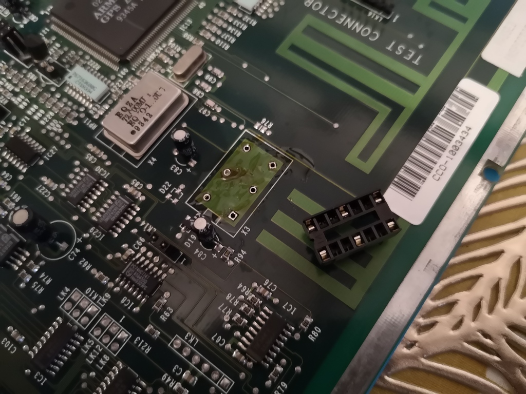
Next I used good quality solder wick along with some flux to remove the excess solder from the socket footprint for X3 (the location on my A3010 where the sysclk clock can be fitted). I find the best way to do this is to apply flux, add new solder and they use the solder wick to remove it. If it doesn’t all go (like the higher middle location in the photo above), try from the other side (after adding extra flux). If it still doesn’t clear, add more fresh solder (even though this is counter intuitive) and start again. Take your time and don’t keep your iron on the board for too long. Also, don’t set the iron too hot. Around 300 degrees C should be enough, certainly no more than ~330 degrees C.
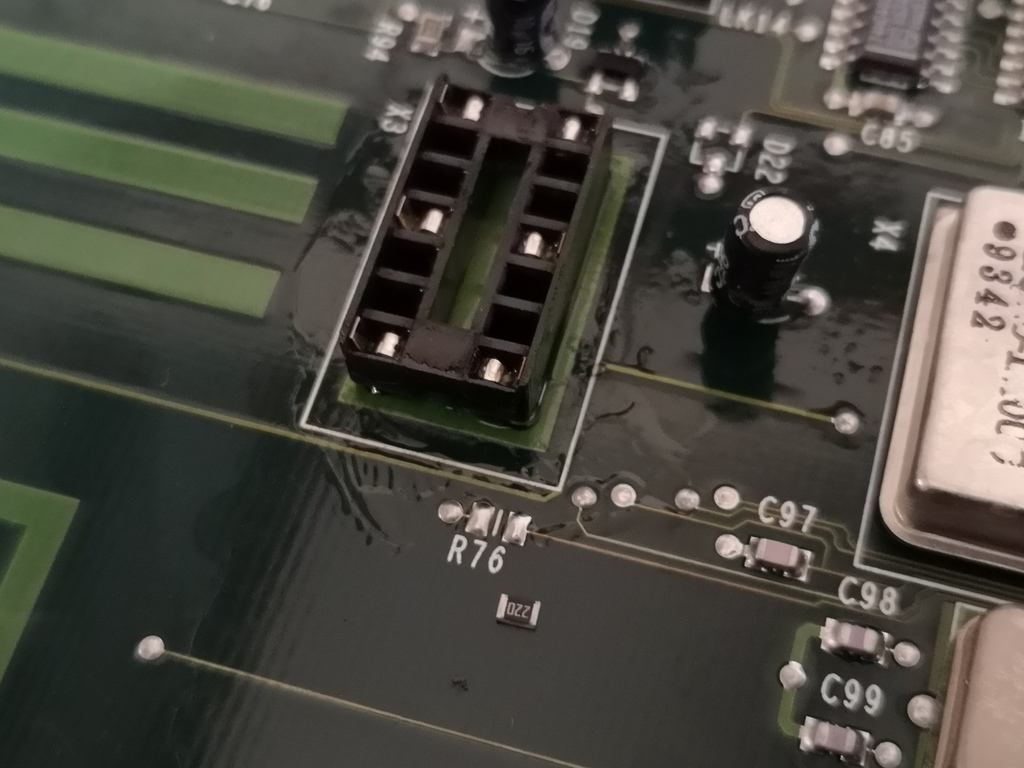
Once all 6 holes have been cleared of solder, you can install the socket (taking note of the notch on the socket and on the silkscreen). I tend to tack one corner first, then with the socket downwards, place my finger on the socket and touch the iron to the single fixed pin so that it reflows and the socket sits flush on the surface of the PCB. Visually inspect before doing the same with the diagonally opposite pin… and if you’re happy it is installed properly, solder the other pins.
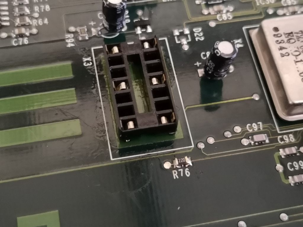
R76 then needs to be fitted as above. First clear the pads of old solder using a bit of flux and solder wick. As mentioned, the 220 label means that this is a 22R resistor. To solder this, I place a small amount of solder on the pad closest to my soldering iron hand, and then briefly remelt this solder while using tweezers to push one end of the resistor into the solder and the whole thing into place. I then solder the other end, before applying a small amount of flux to each pad and reflowing them briefly to tidy them up. Don’t worry too much if it is scruffy, as long as the solder doesn’t bridge the two pads.
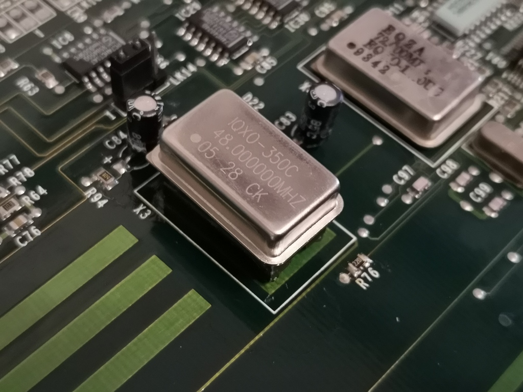
Fit a clock into the socket, taking care to note pin 1 (shown above by a dot next to “05”) and align it at the end with the notch in the socket and silkscreen. Note that if you use a shorter DIP8 style clock, you need to make sure that pin 1 is in the same location as with the DIP14 part. This means that the clock would be at the far end of the socket from R76.
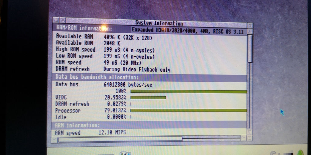
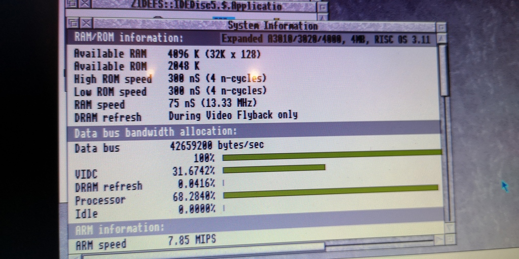
With the 48MHz clock above fitted, the A3010 ran at 48/3 = 16MHz, a 33.3% speed boost. I also later installed a 54MHz clock to give an 18MHz clock speed.
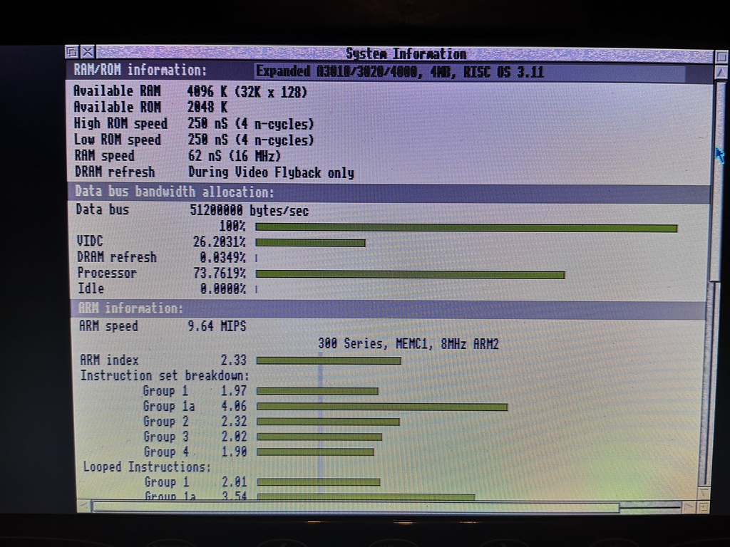
As I am using a RAM module rated at 60ns, 16MHz is within specification for the RAM, and 18MHz represents a very slight overclock (55ns).
Note that interestingly, if you remove the clock and just leave the socket empty, your A3010 will return to its default 12MHz – this modification is trivial to “turn off”.
Turbo Mode
After having overclocked my Acorn, I started thinking. The DIP14 clocks are enormous, especially compared to more modern surface mount clocks that are functionally identical. I decided that I could probably fit 2 or 4 clocks on a small PCB that fit into the space envelope of the original part! A bit more investigating and I found that a commonly available 7x5mm clock package would fit one per side on a board the size of the standard clock package, with a SPDT switch (or header for a remote switch), allowing you to pick your clock speed.
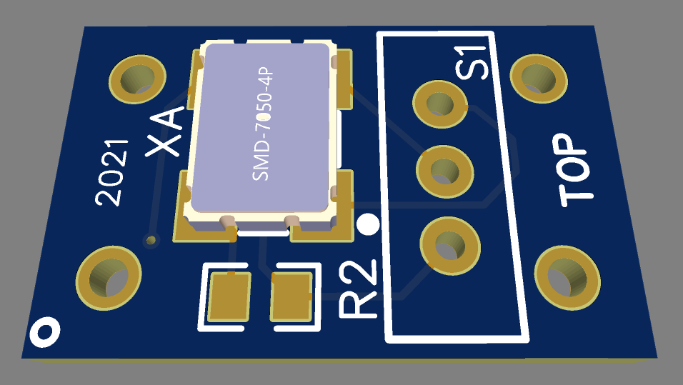
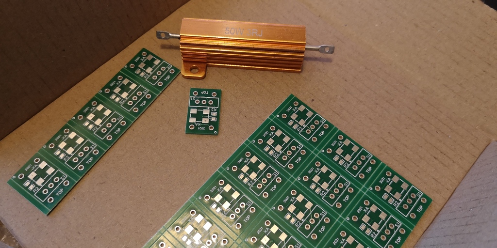
I created a schematic and board layout and ordered some boards to test the idea. A couple of weeks later they arrived and I made one up to test during my lunch break.
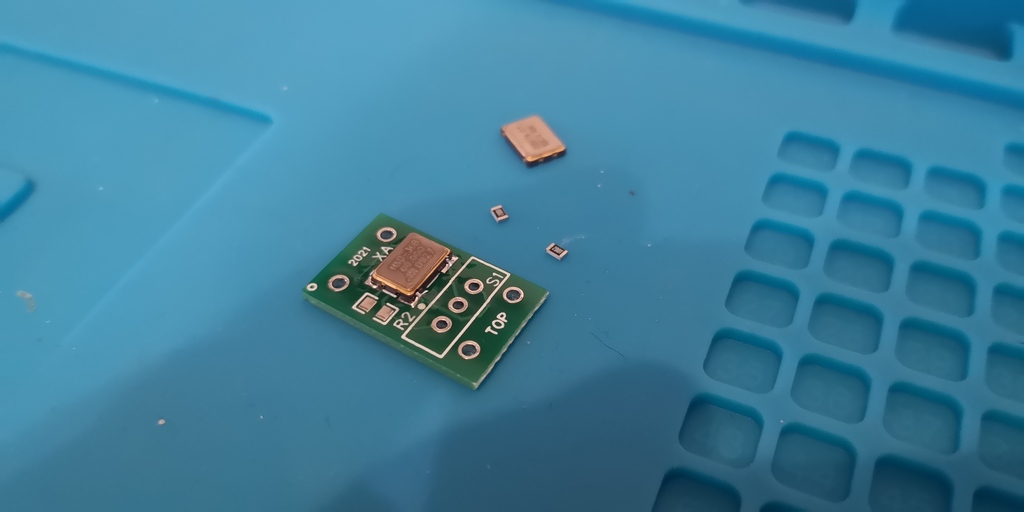
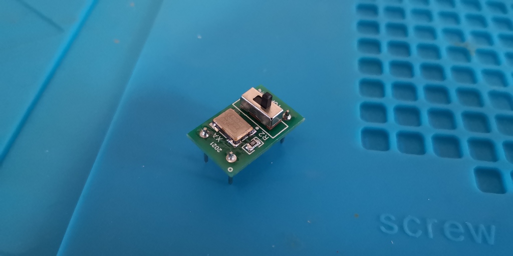
This test device is fitted with a 50MHz and a 60MHz clock, which results in a processor and RAM speed of 13.33MHz and 20MHz respectively, dependant on the position of the switch (in the current design, as photographed above, towards the camera selects the upper clock, and away selects the lower clock).
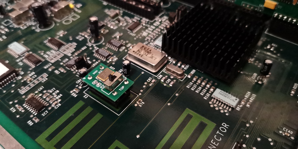
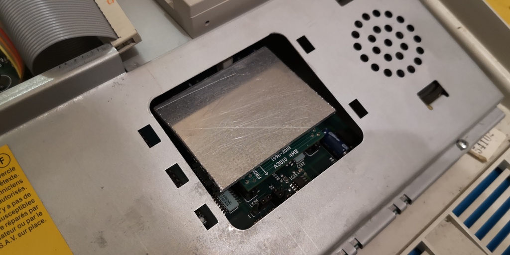
The excellent news is, it works! Note that by this stage I had fitted a standard 40x40mm heatsink. I also fitted a rectangle of aluminium to the RAM.
Both heatsinks were attached using a thermally conductive silicone glue, as I did not want them coming free inside the case.
The photo above shows the A3010 running with the switch selecting the 60MHz clock and the following photo shows with the 50MHz clock selected.
I do not advise switching the switch while the computer is running as it is likely that there will be some unpredictable states as the switch changes position due to switch bounce and the speed at which the two clocks respond. It is very likely that both clocks might be active at the same time and cause a crash.
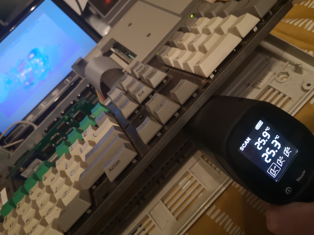
To test the 20MHz overclock, I left the Molecule example running at maximum (unrestricted) speed for over an hour. The SOC temperature peaked at about 29 degrees C (in the photo I’m not hitting the right place on the heatsink, down between the fins).
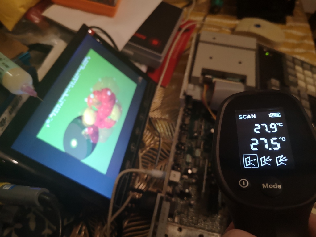
The RAM, to my surprise, was cooler at approximately 25 degrees C.
Next Steps
My intention is now to build a second PCB with a 60MHz and a 72MHz clock. This gives 20MHz and a 24MHz processor and RAM speed. My preference would be for 18MHz and 24MHz, but I don’t have a 54MHz SMD clock. With this PCB, I will attach flying leads and mount a three way switch on the podule blanking plate, with the correct wiring and switch, I’ve worked out that I can disable one, the other, or both clocks, giving me the ability to select 12, 20 or 24MHz. The best bit is that I wont have to keep dismantling my computer!
Stardot thread : https://stardot.org.uk/forums/viewtopic.php?f=16&t=21639